
Different Types of PCB Through-Hole and SMT Assembly Processes
PCB Through-Hole and SMT Assembly Processes
PCBs are a vital component of electronic devices. They’re used to connect components and create a circuit board that’s then able to transmit signals to perform the desired function. There are various methods of PCB assembly, but the two most popular are through-hole and surface mount technology (SMT). Both have their merits and demerits, but each offers a different type of assembly process. It’s important to know which process is best for your design and application.
The THT assembly process involves inserting components through holes in the pcb smt assembly and soldering them into place. It’s ideal for larger components that require a mechanically stable assembly. It’s also ideal for applications that must withstand high-stress mechanical stresses, high power, or both. It can also handle higher connection densities because the connections are inserted through the board, rather than being placed on top or back of the circuit boards.
The SMT process is an alternative to the THT assembly method and has a number of advantages over it. For starters, it’s much quicker and more efficient. The process also allows manufacturers to produce more complex products at a lower cost than THT assembly. This is because SMT assembly requires fewer steps and doesn’t require the use of drilled holes that must then be filled with solder.
Different Types of PCB Through-Hole and SMT Assembly Processes
To begin the SMT assembly process, a stencil is placed on the PCB and then the component placement phase begins. A pick-and-place automatic mechanism is then used to carefully place small electronic components on the PCB, according to predetermined locations on the PCB, or by hand. The resulting assemblies must then be visually inspected to ensure that all components have been placed correctly. This is a crucial step because any errors in this phase can cause costly and time-consuming rework.
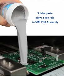
After the component placement phase, the assembled PCBs are then sent to a reflow soldering machine (also called a reflow oven). This is where the components are heated up so that the solder paste melts and bonds the component with the PCB. Once the reflow is complete, the assembled PCBs are then allowed to cool down so that the joints can solidify.
Once the reflow and inspection processes are finished, the assembled circuit boards can then be sent to an automated optical inspection machine (AOI). This is where a 3D optical system looks for any defects in the solder joint quality and the position of the component. This is another critical step because if any defects go unnoticed and the component is soldered to the wrong place, the result can be catastrophic.
After the AOI inspection, the circuit boards are then ready to be shipped and sold. This is a critical step because the faulty circuit boards can ruin an entire batch of production. It’s also because a faulty circuit board can compromise the quality and performance of a final product. To avoid this, all assembled PCBs are thoroughly tested and cleaned before they’re shipped.