
How Are Electrical Circuit Boards Assembled?
Electrical Circuit Boards Assembled
Circuit boards are the heart of electronic equipment such as cell phones, TVs and Blu-ray players. They contain a thin layer of conductive material on an insulating board called a substrate and hold tiny electronic components connected to these conductors through soldering. Assembling a circuit board requires meticulous attention to detail in order to ensure proper function and avoid common mistakes such as a short circuit, which can damage the components and the board.
The first step in assembling a PCB is to apply the component footprints to the PCB layout. This is done using the CAD software that was used to create the layout. After the footprints are in place and the net connections are imported from the schematic, the physical layout of the board begins. This involves rearranging the footprints to meet the mechanical requirements of the board, as well as routing the traces. This is an important step and one that requires experience to be successful. It is crucial to route the traces correctly so they do not cross areas of excessive noise that would degrade the performance of the board.
Once the layout is complete, the circuit board undergoes a series of fabrication processes to prepare it for assembly. This includes drilling holes for the component leads and vias, which are plated with copper electroplating to provide the electrical connection between different layers of the circuit board. It is also possible to add a layer of silkscreen that provides labels for the components on the circuit board. This is useful for identifying components, especially those that may need to be replaced if they are not functioning properly.
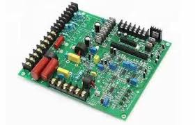
How Are Electrical Circuit Boards Assembled?
Next, the conductive pattern of the circuit board is created by depositing a layer of copper on the substrate. This can either be a copper foil layer or a full copper coating. This layer serves as the PCB’s “blueprint,” and it carries signals to and from the components, much like your nervous system carries information between your brain and your muscles.
Surface-mount technology is used for most of the smaller components, such as resistors and diodes. These are placed directly on the surface of the board, which is often covered with a protective layer known as a solder mask.
Thru-hole technology is used for larger components that have wires that pass through the holes on the board and are soldered on the other side. These components include ICs and power and ground planes, which must be carefully positioned to ensure good conductivity while avoiding any overheating issues.
Once the components are in place, the electrical circuit board is sent through a reflow oven to melt the solder paste. This process heats the components to a temperature that allows the solder to bond with the pads on the circuit board and form a solid, electrical connection. The board is then cooled to solidify the solder and finish the assembly process. It is then ready for inspection and testing. If the board is found to be functional, it can be shipped to customers.