
How are prototypes made in circuit board assembly?
prototypes made in circuit board assembly
PCB prototypes are essential for ensuring that the final product will function properly and meet design specifications. This process also identifies potential issues that can be addressed in the design before going into production. This will allow for smooth transition from prototype to production without costly redesigns or delays in time-to-market.
A circuit board’s assembly is done by placing components and connecting them to one another using soldering techniques. This is a critical step in determining the correct size and dimensions of the circuit board and its overall performance.
Before proceeding to the assembly phase, a schematic diagram of the circuit board assembly must be created. This will outline the layout and basic connections of all the components and their relationships. This stage is a crucial part of the design process, and it is often used to communicate key information like component sizes, mounting holes, and electrical connections to other teams involved in production. This will also help the design team make informed decisions and avoid expensive mistakes during production.
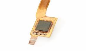
How are prototypes made in circuit board assembly?
The next phase involves transferring the schematic diagram to a computer-aided design (CAD) software program. Typical programs include Eagle, Altium, Cadence, and KiCad. These programs use Gerber files to define the structure of a circuit board, including the copper layer patterns, drill holes, solder masks, and silkscreen details that will be used during fabrication. It is important to ensure that the resulting bare PCB is consistent with the schematic and follows manufacturing rules, such as clearance and trace width guidelines.
Depending on the complexity of the circuit, there are various options for fabricating a bare PCB. Common substrate materials include FR-4, polyimide, and glass-epoxy laminates. The choice of substrate depends on the performance requirements of the circuit and other considerations such as cost, temperature, and handling. Other important factors in the bare PCB fabrication process are component placement, board thickness, and the ability to pass a quality control inspection.
After the bare circuit board is fabricated, it must go through a debugging and testing process to ensure that it meets the requirements of the original design. Typically, the circuit board is tested for continuity, functionality, and electrical connections. If any issues are identified, it is necessary to recheck the design or assembly process.
The most important benefit of a pcb assembly prototyping is that it enables the engineer to test and validate the design before investing in costly tooling and volume production. This is important because a prototype can be used to evaluate assembly and debugging processes. It can also help pin-point cost-saving adjustments, which can be difficult to determine during the actual design process. This can be a significant advantage, especially in projects that have tight timelines. Ideally, the prototype will serve as a test bed for all possible configurations of components, parts, and materials to optimize performance and cost. Ultimately, the prototyping process can significantly reduce production costs and increase efficiency by identifying potential design flaws. These issues can be resolved through iterations of the prototype to produce a high-quality, reliable final product.