
How does an HDI printed circuit board affect product reliability?
HDI printed circuit board affect product reliability
A printed circuit board is an essential component in a wide range of electronic devices. It is responsible for carrying electrical signals between different components. It also provides space for other important functions such as power distribution, grounding and signal isolation.
PCBs are manufactured using various materials and surface finishes, depending on their application. These can be chosen for their coefficient of thermal expansion (CTE), performance under stress, dielectric constant and low/ultra-low loss characteristics. An hdi printed circuit board is an advanced version of a standard printed circuit board with more layers and smaller features. These can be used in products that require high levels of reliability and performance, especially those that will operate in extreme environments or in hazardous conditions.
In a conventional multilayer PCB, the copper layers are separated by partially cured laminates and stacked together like a book with layers of prepreg on top and bottom. During the lamination process, these layers are heated to liquify the prepregs and stick them together. A single stack-up can have many numbers of laminations, depending on the design. The more layers, the more expensive the board will be. For a more complex stack-up, a blind and buried vias structure requires multiple successive laminations.
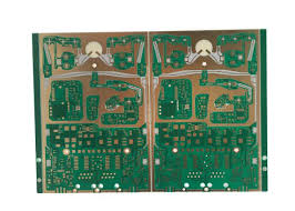
How does an HDI printed circuit board affect product reliability?
Compared to traditional PCBs, an HDI printed circuit board has greater density and a lower minimum pitch, resulting in less wire length. This means that the components on the board can be placed closer together, enabling improved electrical performance. The shorter distance between components can reduce signal loss and crossing delays. In addition, a more stable voltage rail and less stubs are possible, as well as a better distribution of capacitance.
The higher packing density achieved by HDI technology allows for more pins and connections to be packed onto the board, reducing the overall size and weight of the product. This allows for faster transmission of signals, which in turn improves device performance and reliability. In addition, a reduced footprint makes it easier to solder and assemble.
An HDI PCB can be used in a wide variety of devices, including mobile phones, laptop computers, digital cameras and 4/5G network communications equipment. They are also a common feature in medical devices, including monitors and surgical instruments. They are even found in military applications, such as smart munitions and radar systems.
Although HDI PCBs are highly reliable, there are a few things to keep in mind when designing for them. For example, it’s important to account for drill-to-copper clearance, which is often much more limited than the standard value of 7 to 8 mils. This can cause problems with automated tools that do not take these limitations into consideration. Another important factor to consider is the thickness of the copper layer. Choosing thinner copper can help reduce the cost of the finished product. Finally, it’s critical to choose a manufacturer that can handle the extra time required for laser drilling and multiple lamination cycles. Otherwise, you could run into lengthy lead times, which can impact your project’s development schedule and delay shipment dates.